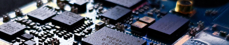
The way an electronic device works is defined by the complexity of their built-in circuits, which are as important as the printed circuit boards (PCBs) where they are installed. They both are the pillars of today’s electronics, as just about every electronic device needs a PCB to be fully integrated.
GCE specializes in the design and manufacturing of printed circuit boards; a job that is essential for the technology society we now live in, even if its final outcome (the board itself) is hardly ever acknowledged and appreciated — except for the professionals of the industry.
Types of printed circuit boards
Printed circuit boards and technology advances have evolved hand in hand, giving rise to the design and production of different types of PCB according to the demands that have emerged over the years.
Below you will find the most common types of printed circuit boards and their main features:
Single-layer printed circuit boards
This design is entirely based on one single layer of dielectric substrate and one layer of conductive copper. Such components are welded on one side so they can be produced in a more simple, cost- effective and faster way. Nowadays, different electronic devices - calculators, radios or even printers - include them.
Double-layer printed circuit boards
Even if this kind of boards also feature single-layer dielectric substrates, they are covered with copper on both sides. Their metallic holes and threads allow to connect both sides, enhancing interactions among components. Thanks to these improvements, more complex equipment can be operated, namely LED lighting systems, air-conditioning systems, amplifiers, simple electronics for automobiles, and also basic phones.
Multi-layer printed circuit boards
When printed circuit boards have more than two conductive layers, they are referred to as “multi-layer”. The different conductive layers are put in between those including dielectric materials. By connecting them through metallic holes and threads, the number of possible interconnections increases exponentially, and so do the complexity and ability to miniaturize the board. They offer several applications and include advanced electronic developments — for example, data-storage systems, meteorological analysis equipment or even satellite systems, to name a few.
Rigid printed circuit boards
When we talk about rigid printed circuit boards, we are referring to those that cannot be bent or deformed, meaning that they use rigid substrate. This kind of PCB — which can be also single-layer, double-layer, or multi-layer — stands out for its resistance. Often, they can be found in GPS systems, cell phones and temperature sensors.
Flexible printed circuit boards
On the other side, flexible printed circuit boards can be easily deformed and bent, hence the manufacturing process is more costly as compared with its rigid counterpart.
They also bring more benefits. For instance, they are much lighter and can be placed in small non-flat areas, while being resistant to different weather conditions. None of these features is applicable, however, to rigid boards.
Rigid-Flexible printed circuit boards
The technological progress has opened the door to mixed solutions, that is, one given device combines the features of a rigid PCB and those of a flexible PCB. Curiously enough, the combination of properties of this boards makes them smaller, but also more aerodynamic and lighter. These are currently included in cell phones, automobiles or even pacemakers.
IPC standards: a good-practice guide to optimal results
When designing a printed circuit board, it is essential to rely on IPC standards or international regulations on the design of printed circuits and electronic products.
These are not the only standards covering electronics: ISO standards have to do with processes, design and product development; ITU standards aim at standardizing telecommunications; IEC standards are targeted for the certification of electronic products, etc.
As for IPC, it is a worldwide association that aims at paving the way for electronics manufacturers - including those in charge of producing printed circuit boards.
IPC standards gather the protocols making up a guide of the best practices in terms of design, production, assembly and PCB inspection. Meeting IPC standards means that the highest quality levels are reached during this process.
Even if they are not compulsory, relying on IPC standards brings about a great deal of advantages, among others:
- IPC standards are accepted, ensuring that they are in line with the best practices in the
industry. - It shows a company’s commitment and excellence in this sector.
- In general, it helps PCB designers do their job.
- It saves manufacturers and users interpreting issues.
- These standards make information exchange easier.
- They promote the development of products of higher quality.
- They are useful in reducing time in every development process.
- They also consider sectors like manufacturing and environment.
- Finally, they can be used to launch high-quality products in less time.
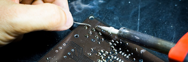
Phases of a PCB manufacturing process
Producing PCBs involves several chemical and mechanical processes that may vary depending on what we are manufacturing — single-layer, double-layer or multi-layer boards. In general terms, we are trying to reproduce a design with conductive elements - tracks, holes, grounding, contact or solder pads - on copper foils put together with dielectric material. Therefore, these processes consist of adding or removing copper, and on removing dielectric material. If we are dealing with a multi-layer circuit - which is the most complex type of board - the process is as follows:
- Application of photosensitive film to inner layers.
- Etching process (removal of copper excess).
- Application of an oxide film and lamination.
- Drilling and application of a conductive layer to the holes.
- Application of external photosensitive film and electroplating.
- "Strip-etch-strip" process (removal of copper excess and tin).
- Application of solder mask and legend.
- Application of final finish to those elements that are not covered by the mask (contact and dissipation pads, pads used to weld components, etc.)
Inspection and verification stages
One of the quality requirements set by the IPC standards and by the company itself is that circuits must be subject to inspection and verification at different stages of the manufacturing process. Some routine inspections performed are as follows:
- Thickness of the hole metallizing.
- Layers properly lined up in multi-layer boards.
- X-ray measurements of the thickness of surface finishes (Chemical silver and ENIG).
- Automated Optical Inspection (AOI)
Most specifically, AOI technology allows us to check in an easy and accurate manner that the design of an inner or outer layer of a circuit has been properly transferred to the copper layer during the manufacturing process. With this machine, we can check the dimensions of the elements, gaps, centering of holes between layers, and, especially, we can check shorts (copper elements connecting two elements that are isolated in the design) and opens (lack of copper provoking the isolation of two points that were supposed to be connected based on the design).
Printed circuit boards or PCBs are one of the most important elements of today’s technology. GCE is at the forefront of every design and production process of these and many other components so that our clients can have products of the highest quality.
Do you want to be up to date with our news and the most relevant developments of the industry? Do not miss out on any news of our blog and newsletter!
There, we will share with you technology solutions for different areas, such as telecommunication and TV infrastructures, hospitality, professional LED lighting, and also social and healthcare installations.
LEAVE THE COMMENT